September 22, 2022
This change was made in a bid to attract more international players to set up production bases in the country
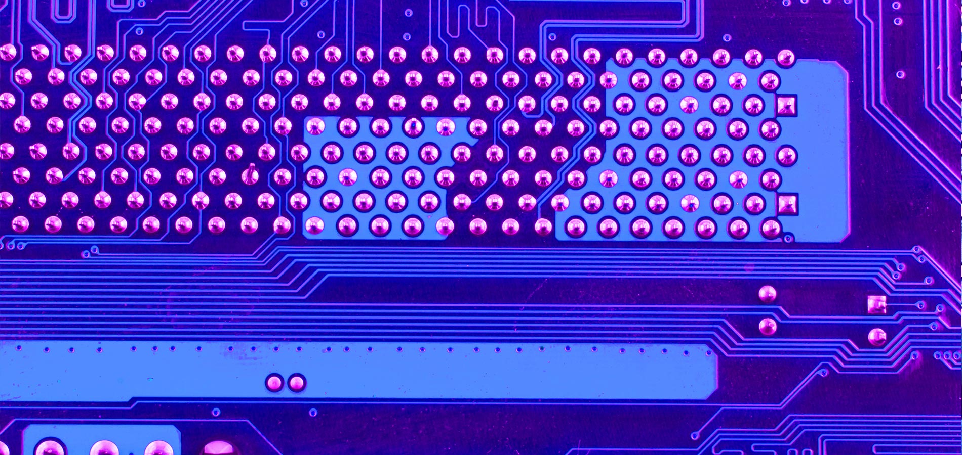
India’s semiconductor industry was valued at US$ 27.2 billion last year
The market is expected to grow at a CAGR of 19% to reach US$ 64 billion over the next four years
This move is expected to further increase the interest and create additional proposals that have been in discussions over the last 4-5 months
The Indian government has changed the INR 76,000 crore Product Linked Incentive (PLI) scheme by being willing to bear 50% of the project costs across all categories of factories, in a bid to attract more international players to set up production bases in the country.
According to media reports, the PLI scheme announced in December 2021, was set up to provide a diverse range of monetary support (ranging from 30-50%) to various departments of manufacturing semiconductors and displays in India. Earlier, companies setting up fabs to manufacture 28-45 nm node chipsets and 45-65 nm chips were eligible for 40% and 30% of the project cost reimbursement. TFT LCD/ AMOLED displays, on the other hand, included reimbursement of up to 50% of the project cost with a cap of Rs 12,000 crore for each fab.
Now, the amount of support (reimbursement) has been uniformly set for all components to 50%. The reason behind this incentive is to attract players across the entire semiconductor ecosystem.
Government officials said that the outlay will remain the same, however, the revision of monetary support for the semiconductor policy will attract investment opportunities across various departments, such as namely silicon and compound fabs, packaging units, display fabs, and design and innovation ecosystem. This move is expected to further increase the interest and create additional proposals that have been in discussions over the last 4-5 months.
They further added that an investment of INR 2 trillion will be brought into the country by 2025 as international companies are planning to explore India as a destination for semiconductors. India is positioning itself as among the most attractive destination in Asia for “all things electronics and semiconductors”.
The reports mentioned that India’s semiconductor industry was valued at US$ 27.2 billion last year, and is expected to grow at a CAGR of 19% to reach US$ 64 billion over the next four years.
As per the officials, the trailing edge nodes which fall into the frequency of 65 nm and beyond have a large potential in contributing to the high-power and automotive segments. The tweaks in incentives are expected to attract more proposals from these segments.
Source: Economic Times